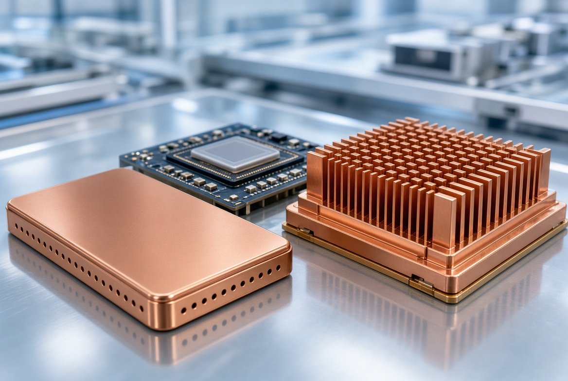
Effective thermal management stands as a critical requirement in modern microelectronics design and manufacturing. As devices continue to shrink in size while increasing in power density, the ability to efficiently dissipate heat becomes essential for maintaining performance, reliability, and longevity. Excessive heat accumulation can lead to reduced operational efficiency, accelerated material degradation, and outright failure of sensitive semiconductor components.
Engineers and designers therefore prioritize materials and structures that combine high thermal conductivity with carefully controlled coefficients of thermal expansion to match the properties of silicon, gallium arsenide, gallium nitride, and related compounds. In Watsonville, California, specialized manufacturing capabilities support the production of advanced composites that address these exact challenges across optoelectronics, high-power lasers, radio-frequency amplifiers, and high-brightness lighting systems.
The Importance of Controlled Expansion Materials
Microelectronic devices generate significant heat during operation, particularly in high-power applications such as semiconductor diode lasers, microwave amplifiers, and power electronics modules. Traditional pure copper heat sinks offer excellent thermal conductivity but expand and contract at rates that differ substantially from those of semiconductor dies. This mismatch creates mechanical stress during temperature cycling, which can crack solder joints, delaminate interfaces, or fracture the die itself.
Controlled expansion composites solve this problem by blending refractory metals such as tungsten or molybdenum with copper. The resulting materials deliver thermal conductivity values typically ranging from approximately 150 to 220 watts per meter-kelvin while providing coefficients of thermal expansion that closely track those of gallium arsenide or gallium nitride across a wide temperature range. Stability of the expansion coefficient remains consistent from room temperature well beyond the melting points of common solders, ensuring reliable performance during assembly and subsequent operation.
Tungsten-Copper and Molybdenum-Copper Composites
Among the most widely adopted solutions are tungsten-copper and molybdenum-copper composites produced through powder metallurgy techniques. A porous skeleton of sintered tungsten or molybdenum is infiltrated with molten copper under carefully controlled conditions. This process yields a highly homogeneous microstructure in which thermal conductivity remains essentially isotropic, meaning heat flows equally well in the x, y, and z directions.
Homogeneity also contributes to predictable mechanical behavior and consistent plating quality, even on narrow features or complex geometries. Different weight ratios of the refractory metal to copper allow precise tuning of the expansion coefficient. For example, a ninety-percent tungsten and ten-percent copper composition often exhibits an expansion coefficient near 6.2 parts per million per kelvin at room temperature, closely matching gallium arsenide, while slightly higher copper content increases conductivity at the modest expense of a higher expansion value. These materials find extensive use as spacers, submounts, bases, and flanges in laser diode packages, optical benches, and amplifier assemblies.
Applications in High-Power Semiconductor Lasers and Optoelectronics
High-power semiconductor lasers used in industrial material processing, medical systems, and defense platforms place extreme demands on thermal management. Laser bars can generate heat fluxes that quickly degrade performance or destroy the device if not removed efficiently. Tungsten-copper spacers mounted between the laser bar and a larger heat sink provide a thermally matched interface that conducts heat away while minimizing stress.
Exceptional surface flatness, tight dimensional tolerances, and controlled edge radii support reliable soldering and long-term reliability. Similar principles apply to high-brightness light-emitting diodes, where plated tungsten-copper wafers enable wafer-level packaging approaches that reduce manufacturing costs while maintaining efficient heat extraction. In radio-frequency and microwave amplifiers based on gallium arsenide or gallium nitride, composite bases and flanges transfer heat from the active devices into the chassis or cold plate without introducing excessive mechanical strain.
Manufacturing Precision and Surface Engineering
Beyond bulk material properties, the final performance of a thermal management component depends heavily on machining accuracy and surface preparation. Advanced facilities achieve flatness values measured in fractions of a micrometer per millimeter, surface roughness as low as a few hundredths of a micrometer, and dimensional tolerances measured in tens of micrometers. Such precision ensures intimate contact with the semiconductor die and with subsequent heat-sinking layers.
Dedicated plating processes deposit gold-tin or other solderable layers of consistent thickness and composition, even across intricate features. Brazing capabilities further allow attachment of the composite materials to ceramics, creating robust optical benches that integrate lasers with lenses and other photonic elements. These manufacturing strengths support both standard product forms and highly customized geometries required by demanding aerospace, telecommunications, and scientific instrumentation applications.
Advantages for Reliability and System Longevity
The combination of high isotropic thermal conductivity and stable expansion behavior translates directly into improved system reliability. Reduced thermal resistance keeps junction temperatures lower, which in turn slows degradation mechanisms such as electromigration and intermetallic growth. Matched expansion minimizes cyclic fatigue in solder joints and bond interfaces, extending the operational lifetime of the assembly under repeated power and temperature cycles.
In environments where devices must operate at elevated ambient temperatures or under rapid thermal transients, the inherent stability of the composite materials provides an additional margin of safety. Designers can therefore push power levels higher or reduce package size without compromising lifetime targets, supporting ongoing trends toward greater functionality in smaller form factors.
Local Expertise Supporting Advanced Microelectronics
Watsonville, California, hosts specialized manufacturing focused on refractory metal technology and controlled expansion composites for microelectronics. One established provider in the region, Spectra-Mat, Inc., applies decades of powder metallurgy experience to produce tungsten-copper and molybdenum-copper components tailored for laser, amplifier, and LED applications.
The combination of material science depth, precision machining, and plating expertise available in this location supports both prototype development and high-volume production for customers worldwide. Engineers seeking reliable thermal management solutions benefit from the ability to specify exact compositions, geometries, and surface finishes that align with the thermal and mechanical requirements of their particular semiconductor devices.
Future Directions in Microelectronic Cooling
As power densities continue to rise with the adoption of wide-bandgap semiconductors and advanced packaging architectures, thermal management materials must evolve in parallel. Hybrid approaches that integrate controlled expansion composites with microchannel cooling structures illustrate one promising path. By combining the mechanical and thermal matching advantages of tungsten-copper with optimized fluid flow channels, designers can achieve still lower thermal resistance while preserving the expansion compatibility essential for reliability.
Continued refinement of infiltration processes, surface treatments, and joining methods will further expand the design space available to microelectronics engineers. The fundamental principles of balancing conductivity against expansion coefficient will remain central, guiding the selection and application of materials that keep next-generation devices cool and reliable.
FAQs
What makes tungsten-copper composites suitable for thermal management in microelectronics?
Tungsten-copper composites combine the high thermal conductivity of copper with the low expansion and high strength of tungsten. The resulting material conducts heat efficiently while expanding at rates that closely match common semiconductors, reducing mechanical stress during temperature changes.
How does the coefficient of thermal expansion of these materials remain stable?
The homogeneous distribution of copper within a sintered tungsten matrix produces an expansion coefficient that stays relatively constant from room temperature through temperatures exceeding typical solder melting points, ensuring predictable behavior during both assembly and operation.
Why is isotropic thermal conductivity important?
Isotropic conductivity means heat flows equally in all directions, preventing localized hot spots and allowing more uniform temperature distribution across the device. This property arises from the uniform microstructure created by the copper infiltration process.
In which applications are molybdenum-copper composites preferred?
Molybdenum-copper variants are frequently selected for aerospace radio-frequency amplifiers and other applications where a specific combination of expansion coefficient, density, and conductivity provides the optimal balance for the system requirements.
How do precise machining and plating contribute to performance?
Tight dimensional control and superior surface finish maximize contact area with the semiconductor die and heat sink, minimizing interfacial thermal resistance. Consistent plating ensures reliable solder wetting and long-term joint integrity even on complex or narrow features.
Can these materials support wafer-level packaging approaches?
Yes, plated tungsten-copper wafers in sizes ranging from two to six inches enable efficient thermal management at the wafer level for high-brightness LEDs and related devices, supporting cost-effective manufacturing while maintaining thermal performance.